


Imec and UTAC have developed a unique process for the wafer thinning and backside metallization of highly stressed GaN-on-200mm Si wafers. This has resulted in a packaged 650V GaN device – smaller than state-of-the-art.
The wide-bandgap material gallium-nitride (GaN) has many advantages over silicon (Si) when it comes to applications in the area of power electronics. With a higher breakdown strength and lower on-resistance, GaN-based power devices can convert power more efficiently than today’s most advanced Si-based devices. Apart from these assets, GaN-based power devices have a 10 – 100 times faster switching speed than Si-based devices, which makes them perform significantly better at the system level. With these properties, the first generation of GaN-based power devices have found applications, such as battery chargers for mobile phones and electric cars, point-of-load power systems, industrial power supplies, DC/DC convertors for servers, and invertors for solar panel connections to the grid, to name a few.
Today, GaN is grown on a variety of substrates, including sapphire, silicon carbide (SiC) and silicon (Si). Si substrates have become attractive because of the lower cost perspective and the ability to use standard semiconductor processing lines. While industry is mainly working on wafers with diameters of 150mm, imec has pioneered the development of the technology on 200mm Si wafers.
Fabricating GaN-on-Si power devices on 200mm wafers is however challenging: because of the larger diameter and targeted higher voltage range, the wafer bow gets worse. The fundamental difficulty is caused by the mismatch in lattice and especially in thermal expansion coefficient between the GaN/AlGaN layers and the Si substrates. The AlGaN buffer, which is required to ‘bridge’ the Si and GaN lattices, is grown at high temperatures. During cool down, the wafer gets warped, and the highly stressed wafers can easily break or exhibit micro-fractures. By careful stress engineering, imec has enabled a 200mm CMOS-compatible GaN power device platform. With this platform, enhancement-mode power switches and Schottky diodes can be developed, for 100, 200 and 650V voltage ranges.
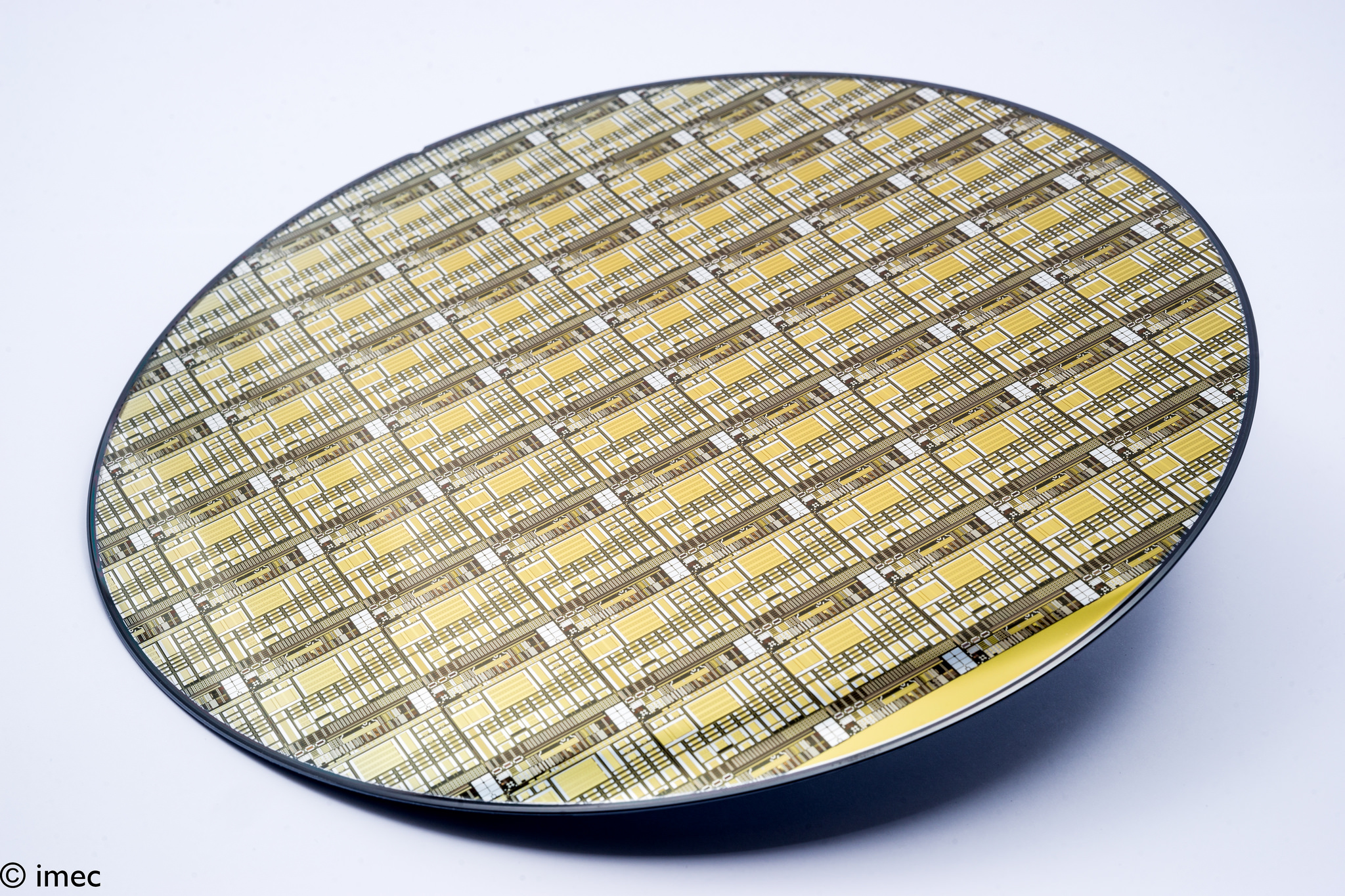
Typical 200mm Si wafer with processed GaN devices
In addition to wafer fabrication, the presence of stress in the wafers also poses challenges during the packaging of these power devices.
Although solutions exist for smaller-sized GaN-on-Si wafers, there is no reliable process for packaging the brittle GaN-on-200mm devices. The development and migration of a GaN-on-200mm Si technology is impossible without a packaging solution. To tackle this challenge, imec has collaborated with OSAT partner UTAC for the assembly of GaN-on-200mm Si technology. Below, Stefaan Decoutere, Program Director GaN Power Electronics at imec, and Nicolo Ronchi, researcher at imec have teamed up with UTAC’s R&D team to list up the challenges, and develop a process and bill of materials for the first, ultra-small, functional packaged GaN-on-200mm Si device.
Packaging GaN-on-200mm Si devices: what are the challenges?
Power devices typically operate at high voltages and high frequencies. In these devices, heat is being generated as a byproduct of operation. The package should therefore provide an efficient path for heat dissipation. For GaN-on-200mm Si power devices, an attractive approach is to thin the Si carrier wafer and subsequently apply back-side metallization. This way, a good thermal and electrical contact between the chip and the package can be established, and uniform heat dissipation can be guaranteed. However, the tensile stress induced by the GaN layer on top of the 200mm Si wafer is strong enough to bow the wafer. And this can lead to breakage during wafer thinning and metallization.
After successful backgrind and backside metallization of GaN-on 200mm wafers, dicing is required, and this process also presents its own set of challenges. Conventional sawing is not possible due to the brittle characteristic of the wafer that can cause chipping and even microcracks. And this urges the need to define and optimize this process prior to packaging.
After dicing, the separated dies need to be mounted into packages. These packages need to be as compact as possible, with an optimized short pin configuration. Compact packages and short pins will not only bring benefits for applications where size matters, they will also reduce the parasitic inductance that is typically caused by the long bond wires and pins. This parasitic inductance is known to severely limit the final speed at which the packaged device can operate. A high thermal and electrical conductive material is also needed to ensure an efficient path between the die backside and the package which is essential for this type of package. Finally, the individual packaged devices are to be soldered onto a PCB with good thermal conduction.
A dedicated process flow
With these challenges in mind, imec and UTAC have developed a unique solution for packaging GaN-on-200mm Si power devices.
For these developments, p-GaN high-mobility-electron devices (HEMTs) were processed on a thick (1,150µm) 200mm Si carrier wafer. On these wafers, a wafer warpage as large as 700 – 900µm was measured after wafer thinning (the warpage being the distortion from the lowest point to the highest point of the wafer), illustrating the difficulty of developing a reliable process flow.
Though there were no issues during wafer thinning, a high warpage post-backgrind process was observed. This is a high concern during the backside metallization of the thinned wafers. UTAC together with their supplier worked on a backside metallization process addressing the high warpage after thinning, and successfully coated a Ti-Ni-Ag layer with a mirror finish. To decrease the level of chipping during die separation, UTAC defined a dicing process that includes laser grooving in conjunction with mechanical sawing. This combined process enables grooved trenches along the sawing streets prior to mechanical sawing. This also removes the GaN buffer along the die edges and results in limited chipping and cracking of the GaN buffer at the surface.
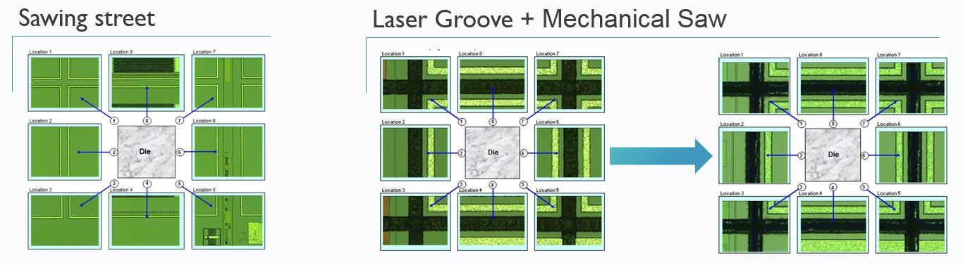
Illustration of the laser groove procedure and mechanical saw, resulting in limited chipping
In a final step, each die is mounted in an industry-standard dual flat no-lead (DFN) package. To meet the requirements for power applications, a highly conductive material was used at die attach, and small pins were provided.
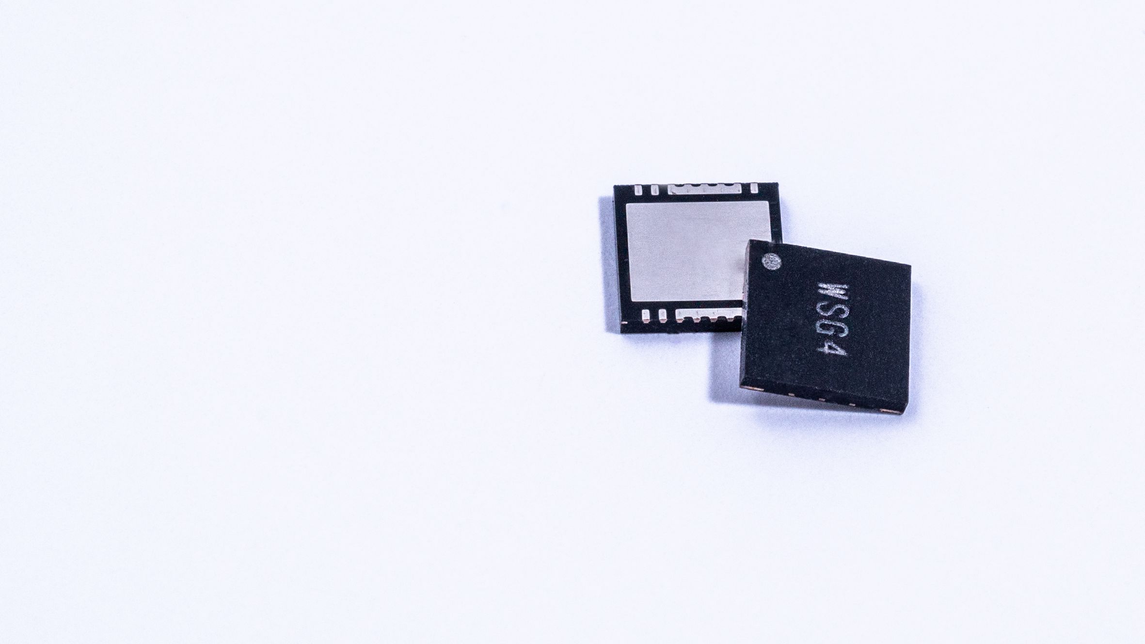
Picture of the 5x5mm2 650V 16A packaged GaN device
A fully functional, compact, 650V 16A GaN packaged device
With a total area of 5x5mm2 and a final thickness of 0.7mm, the resulting packaged devices are smaller than state-of-the-art.
To verify that they operate correctly, standard electrical characterizations were performed. It was found that the packaging process did not impact the operation or stability of the components. The DFN packaged devices can operate at voltages as high as 650V (drain-to-source breakdown voltage) and at 16A drain current, while exhibiting low inductance.
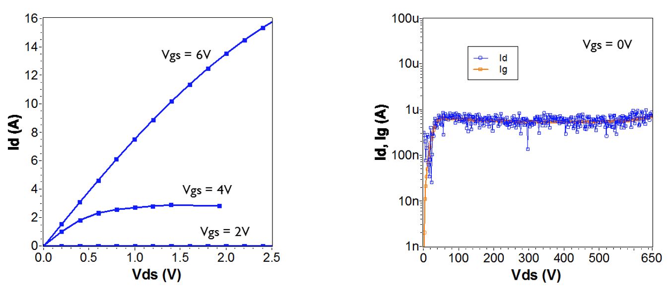
Electrical characterization of the packaged GaN-on-Si devices
The GaN roadmap: new challenges for packaging
With this process flow, imec can now offer its GaN-on-200mm Si technology, all the way from GaN growth and processing to the packaging of the devices. The packaged devices are available as standalone components and can be assembled as discrete components on a common PCB.
Further down the road, imec researchers are looking into other substrates than Si. They explore, for example, substrates that have a better matched coefficient of thermal expansion – such as the recently proposed QST® substrate from Qromis. This substrate promises to enable GaN power devices with operation beyond 650V. Or, alternatively, they look into SOI (silicon on insulator) as a substrate for GaN growth. This material, in combination with trench isolation, allows to monolithically integrate multiple GaN power devices onto a single chip, resulting in smaller and less complex overall systems. Using novel substrates will bring along additional challenges for packaging, which will be the subject of further research.
The research on GaN-on-SOI is part of imec’s Industrial Affiliation Program on GaN power devices. Within this program, imec takes today’s GaN-on-Si technology to a higher level of maturity and reliability, and explores new concepts for next-generation GaN technology.
Ource and full Article : https://www.imec-int.com
Social Media Development addict, Ashley Reyes is specialised on Emerging Techs & Crowdfunding Market. Ashley holds a Bachelor in Marketing and have 5+ years of experience in leader company as Marketing Intelligence Analyst . She is now Chief Community Officer at Athis News.


